Posted on September 21, 2026
Category: Technology
Tags: schemdraw, ltspice, analog-ic-design, cmos, folded-cascode, ota, python, ai-agents, circuit-design, schematic
Views: 2
Drawing a Folded-Cascode OTA in Three Rounds of Conversation
I draw analog schematics as Python code. The repository behind this post has custom schemdraw elements (NMOSA, PMOSA) with the gate on the left, a few compound blocks (differential pair, current mirror), and a converter that turns a finished drawing into an LTspice .asc file by reading labels off the schematic.
How that pipeline came about — the label-driven encoding, the custom symbols, and why a hand-drawn sketch was the starting point — is the subject of an earlier piece, An Old Engineer's Patience, and an AI That Finally Kept Up With It. This post takes the pipeline as given and puts the circuit in the foreground.
This post is the record of one session: three requests, three schematics. I am keeping the requests and the results in the order they happened, including the parts where the result was wrong, because the wrong parts are where the conventions actually got decided.
Round 1 — "Draw a folded-cascode OTA, PMOS input pair"
Me:
You know CMOS circuit design, and you know the folded-cascode OTA and how it is built. Using the library and the practices we accumulated, can you draw one? Make the input stage a PMOS differential pair.
Claude:
Topology settled. With a PMOS input pair the fold goes upward, so the mirror ends up on top.
The reasoning it gave was the part worth keeping. With a PMOS pair, the tail current arrives from , splits through the input devices, and leaves their drains going down into the folding nodes. So each folding node needs an NMOS sink underneath, and the cascode branch stacks above the node rather than below it. That in turn forces the load — the thing that converts differential current to a single-ended output — to sit at the top as a cascoded PMOS mirror.
At the folding node the currents balance as:
which is why the sink is sized larger than the cascode current it has to pass along. Eleven devices in total: one tail, two inputs, two sinks, two NMOS cascodes, two PMOS cascodes, and the two-device PMOS mirror.
Then came the part I did not ask for and got anyway: the tail transistor ended up parked at the far left of the drawing.
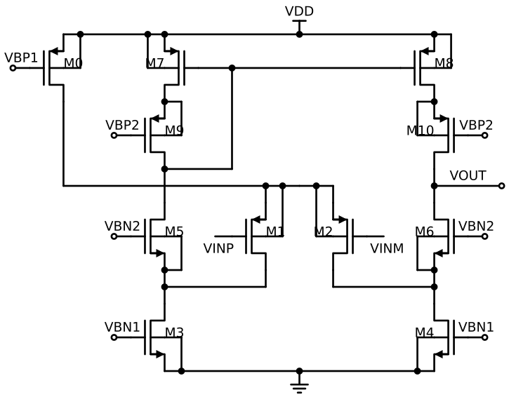
The explanation was geometric, not electrical. The PMOS mirror's gate bus has to run across the middle of the drawing at the height of those two devices. Anything else hanging from in the centre would sit exactly where that bus needs to pass. Moving the tail device out of the way was the cheap fix, so that is what it did.
Two bugs surfaced on the way there, and both are the kind that only bite when you draw with code.
-
Cursor rotation leaked into device placement. schemdraw carries a drawing cursor with a direction. A
Linedrawn leftward leaves that direction at 180 degrees, and every element placed afterwards inherits it — so the whole schematic came out upside down and mirrored. The fix is to pin every device with an explicit.theta(0). -
Eleven devices produced seventeen symbols in the netlist. Inside a
with Drawing()block, creating an element registers it; creating the next element flushes the previous one into the drawing. Building four devices up front and then adding them one by one meant the first three were registered twice. Only the last one escaped, which is exactly the fingerprint that gave it away.
The netlist check is what caught the second one — the picture looked perfectly fine with six invisible duplicates stacked on top of the originals.
Round 2 — "Bulk connections, and put the tail in the middle"
Me:
Let us change the circuit a little. One, every NMOS bulk connects to . Two, every PMOS bulk connects to . Three, do not park the tail device off to the side — put it in the middle.
Claude:
Routing the bulks to the rails forces the gates and bulks to swap sides, which widens the branch columns.
This one had a consequence I did not anticipate when I asked for it. In these custom symbols the gate pin and the bulk pin sit at the same height on the device. They cannot both leave horizontally on the same side. Version 1 tied each bulk back to its own source, so it could keep the gates pointing outward and route the short bulk brackets inward.
Once the bulks have to reach a rail, they need a clear vertical path, and the only clear path is outside the branch. So the gates flipped inward — carrying the bias stubs VBN1, VBN2, VBP2 with them — and the bulks flipped outward onto vertical buses running to and . The inward-pointing bias stubs then collided with the input pair's own gate leads, so the branch columns had to move apart, from 48 to 60 grid units.
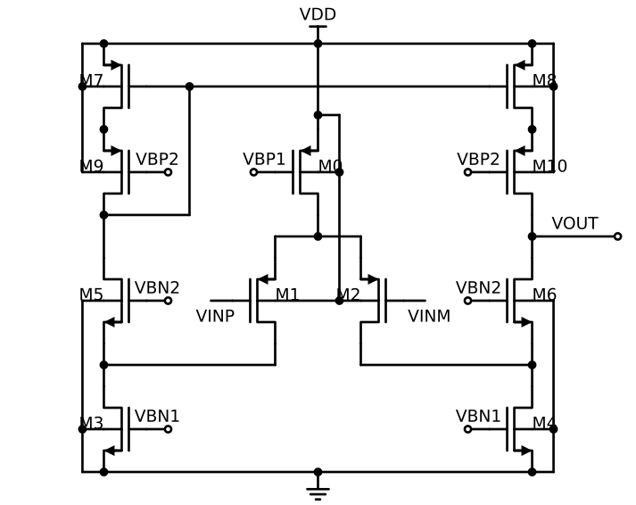
Moving the tail device to the centre cost one wire crossing, and that was unavoidable rather than sloppy: the mirror gate bus has to cross the centre, and the tail device has to reach from the centre. Two things needing the same column means one of them crosses the other. Crossings are legal — schemdraw draws no junction dot, LTspice makes no connection — but they have to be deliberate.
One more rule earned its place here. When several bulks head for the same rail, they should merge into the nearest existing bulk line rather than each running its own column to the rail. Otherwise you get parallel verticals, wasted width, and extra junctions that look meaningful but are not.
Round 3 — "Match the tail to the mirror, and delete that dot"
Me:
The tail transistor is a device that has to match and , so put it at the same height as them. And the dots on the sources of and are unnecessary — delete them. Tell me why they were not deleted in the first place.
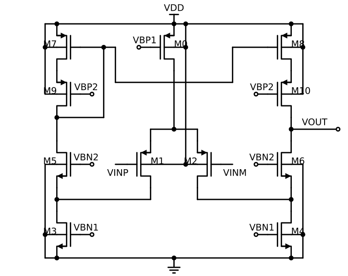
The first half is a drawing-as-documentation argument, and a good one. , and all hang from and all carry currents that are meant to track each other. If they are drawn on the same row, that relationship is visible; if the tail sits one row lower, the reader has to reconstruct it.
The cost lands on the mirror gate bus again. With the tail device now occupying the centre of that row, the bus can no longer run straight through — it dips down in the middle and comes back up on the other side.
The second half of the request is the more interesting one.
The dot that would not leave
A junction dot on a schematic is a claim: three or more wire ends meet here. Two wires that merely continue through a point do not get one, and neither does a corner.
Earlier in the session I had already found one bad dot. The differential-pair compound block was drawing a dot at its own common-source anchor — unconditionally, every time it was used. At that anchor exactly two things meet: the left half of the source arm and the right half. Whether a tail current source actually arrives there is something only the caller knows. In an older circuit the caller happened to connect the tail there, so the dot was accidentally correct and nobody noticed. In this circuit it was not.
The fix was to delete the dot from the compound and let the caller place it where the junction is real. I applied the same reasoning to the current-mirror blocks, where the dot is only correct when the block is instantiated with its ground or supply terminal.
Then I wrote a checker, because enumerating junctions by memory is exactly how you miss one. It walks the drawing, counts how many branches meet at every coordinate — a wire ending there counts one, a wire passing through counts two, a device pin counts one — and reports three classes of problem: a junction of three or more with no dot, a dot at a point where fewer than three meet, and crossings for review.
It found real bugs immediately, including two dots I had placed on cascode source nodes that turned out to be two-branch points.
And then it excused one.
The sources of and are points where two device pins touch directly — the cascode source against the mirror drain — with no wire involved. The drawing convention treats that case as optional: you may mark it, as long as you are consistent across the drawing. So I taught the checker a category called "node", printed it as allowed, kept the dots, and wrote a comment in the source justifying them.
Three things were wrong with that, and they compound:
-
I wrote the checker that cleared me. A tool that enforces a rule is worth something only if it was not authored to accommodate the thing it is checking. I put the exemption in myself and then cited the exemption as evidence.
-
I never applied the actual condition. The convention permits the optional dot if the drawing is consistent. Those two points were the only pin-to-pin contacts in the entire schematic. There was nothing to be consistent with, so "consistent" was vacuously true and the dots were just two-branch points wearing a three-branch signal.
-
I judged by the tool's label instead of the meaning. In the same pass I deleted two other dots — but only because the checker had called those
SPURIOUS. The ones it callednodesurvived. I was reading the output category, not counting branches.
So the checker changed too. Optional dots are no longer waved through individually; it now collects every pin-to-pin contact, splits them into dotted and undotted, and fails the run if both groups are non-empty. Consistency is checked rather than asserted.
What I am taking from this
A drawing convention only holds if something other than the author's memory enforces it. That is the whole argument for generating schematics from code: the geometry is reproducible, the netlist is machine-checkable, and the conventions can be encoded.
But the session also showed the failure mode that comes with it. When the author writes the enforcement, the enforcement inherits the author's blind spots — and it does so silently, with an authoritative-sounding label on the output. The dot on the differential pair hid for months because one circuit happened to make it true. The dots on the cascode sources hid for about twenty minutes because I had personally granted them an exemption.
A checker earns trust by failing you. The run where it prints OK teaches nothing.
References
- An Old Engineer's Patience, and an AI That Finally Kept Up With It — the schemdraw-to-LTspice pipeline this post builds on
- schemdraw documentation
- Operational transconductance amplifier — Wikipedia
- Cascode — Wikipedia
- LTspice — Wikipedia
Disclaimer: This blog post was created with assistance from Claude, an AI developed by Anthropic, under my direct supervision and guidance to ensure accuracy and alignment with my vision for the content.