Posted on September 24, 2026
Category: Technology
Tags: schemdraw, ltspice, analog-ic-design, cmos, symmetrical-ota, ota, current-mirror, python, ai-agents, circuit-design, schematic, netlist-verification
Views: 3
Drawing a Symmetrical OTA in Seven Rounds of Conversation
This is the second circuit I have drawn this way. The setup is the same as in Drawing a Folded-Cascode OTA in Three Rounds of Conversation: analog schematics written as Python code with custom schemdraw elements (NMOSA, PMOSA), a small library of compound blocks (differential pair, current mirror), a converter that turns the finished drawing into an LTspice .asc file, and a checker that counts wire branches at every junction. How that pipeline came about is told in An Old Engineer's Patience, and an AI That Finally Kept Up With It.
The folded cascode took three rounds. This one took seven, plus a follow-up question that ended in a new wiring rule. As before, I am keeping every request and every intermediate schematic in the order they happened, including the wrong ones. One of them is wrong in a way no picture can show.
The circuit
A symmetrical OTA is a differential pair with two diode-connected loads, whose currents are copied out by current mirrors and recombined at a single output.
- is the tail current source; and are the NMOS input pair.
- and are diode-connected PMOS loads.
- and mirror those loads with a ratio (here against , so ).
- and fold the left branch current back to the output with a 1:1 NMOS mirror.
The right branch sources current into the output, and the left branch, after one more mirror, sinks it:
Keep that sign in mind. It comes back in Round 2.
Round 1 — "Draw a symmetrical OTA, NMOS input pair"
Me:
Last time we drew a folded-cascode OTA. Let us do another circuit the same way, using our schemdraw library and the practices we have built up: a symmetrical OTA with an NMOS input pair. Connect every NMOS bulk to and every PMOS bulk to .
Claude:
I will use the library's
NMOSDiffPairfor the input stage. The current-mirror compounds put the diode on the left and run the diode link down the centre line, which collides with the tail — so I will place the mirror devices individually, the way the folded cascode was built.
The layout uses four columns: the output mirrors and on the outside, the loads and inputs and on the inside. The gate bus has to cross the whole drawing, and the tail sits in the middle, so was lifted above the bus and its source wire run down to , crossing the bus once.
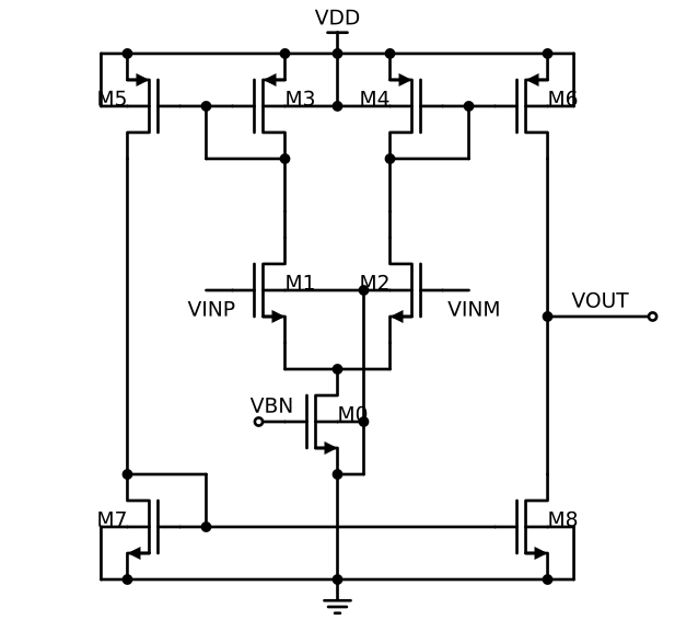
The junction checker passed with two deliberate, unconnected crossings, and the LTspice netlist showed every bulk on the correct rail. By the checks we had, it was done.
It was not. Look at the input labels.
Round 2 — "Keep every version, move the tail down, and why no library?"
Me:
I may write this up later, so do not overwrite intermediate results — keep saving them. Put the tail device at the same height as and . And the current mirrors: was there a reason you did not use our library? Would it not have been easier?
Then, while it was working:
One label is wrong. You should have thought through how and relate to .
The polarity trace is short. Raise the gate of and its drain current rises; carries it, copies it, and mirror it down, and pulls the output lower. So is the inverting input, and its gate is . Round 1 had them swapped.
No tool had caught it. The junction checker counts wires, and the netlist faithfully reports whatever name is written on a gate. Polarity only shows up if someone follows the signal through the mirrors.
The tail move was straightforward. With now sitting on the rail beside and , the bus had to climb over it and come back down, which raised the count of unconnected crossings from one to three.
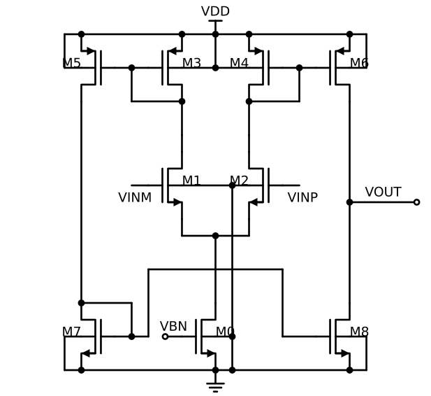
On the library question, the answer came with three reasons: the mirror compound takes one for both devices, so it cannot express the ratio; its diode device is always on the left; and its diode link runs down the centre line where now lives. It also came with an admission — none of this had been tried. The library had been ruled out by reading its code.
Round 3 — "You never tried it"
Me:
For , not using the library is right. For and you could have used it, and you did not even try.
That was fair. The right-hand mirror — diode on the left, output on the right — matched the compound with its default parameters: devices at and , and the diode's drain terminal landing exactly on the input pair's drain. The one real gap, per-device sizing, took a few lines: the mirror compounds now accept w=('10u', '30u').
The left-hand mirror is the mirror image, so the compound was flipped with .reverse().
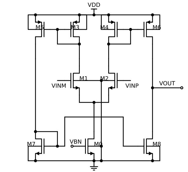
The picture is right. The netlist is not:
M3 N004 N001 VDD VDD PMOSA w=10u l=1u
M5 N001 N001 VDD VDD PMOSA w=30u l=1u
, the big output device, came out diode-connected, and became the output. The drawing shows the diode link landing on the inner device; LTspice was handed a circuit where it lands on the outer one.
The cause is how schemdraw builds a compound. ElementCompound.add() copies each child's drawn segments into the compound's own list, and reverse() mirrors only that copy. The child elements keep their original transforms. The drawing is rendered from the mirrored copy; the converter reads the children. They disagree, and each is internally consistent.
This is the worst category of bug for a drawing pipeline — the kind where the schematic you would show a reviewer is correct. Only the netlist check caught it.
Two fixes were on the table: teach the converter about reversed compounds (the root cause), or add a diode='left'|'right' option to the mirror so nothing needs reversing (smaller, but leaves the trap armed for the next compound someone flips).
Round 4 — "Fix the converter, and look at those labels"
Me:
Go with the converter fix. And the label positions on look slightly different from — check that.
The converter now recomputes the same mirror axis schemdraw used (the compound's center anchor, or its bounding-box centre), mirrors every child coordinate about it, and tracks how many reversed compounds enclose a device so the LTspice symbol gets the right orientation. A passive part inside a reversed compound now raises an error instead of being silently misplaced.
The labels were a second, separate schemdraw behaviour. Mirroring a compound moves each text anchor to the other side, and is supposed to swap its alignment too — but it skips that swap for text with rotation_global set, which is exactly how device labels are drawn. So a label that should read outward from the pin ended up reading back across the gate. A quick inspection showed it directly: after reversal, a label at was still right-aligned. The library compounds now share a small base class that performs the missing swap.
One more cleanup: the line had been drawn across the tops of the inner bulk brackets, doubling up wire. It now spans only the gap between them.
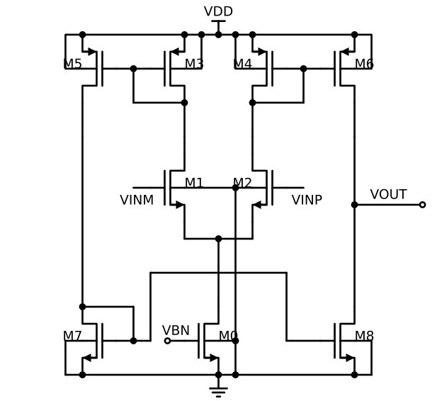
Netlist, checker, and the two previously drawn circuits all passed.
There was a casualty. Checking the fix, I re-ran the Round 3 snapshot script — which imports the live library — and regenerated its figure with the fixed labels, erasing the very failure it was supposed to record. The figure files are generated and not version-controlled, so there was nothing to restore from. The Round 3 script now pins the old behaviour internally so it reproduces the original failure. Snapshot scripts that import a library you are still changing are not snapshots.
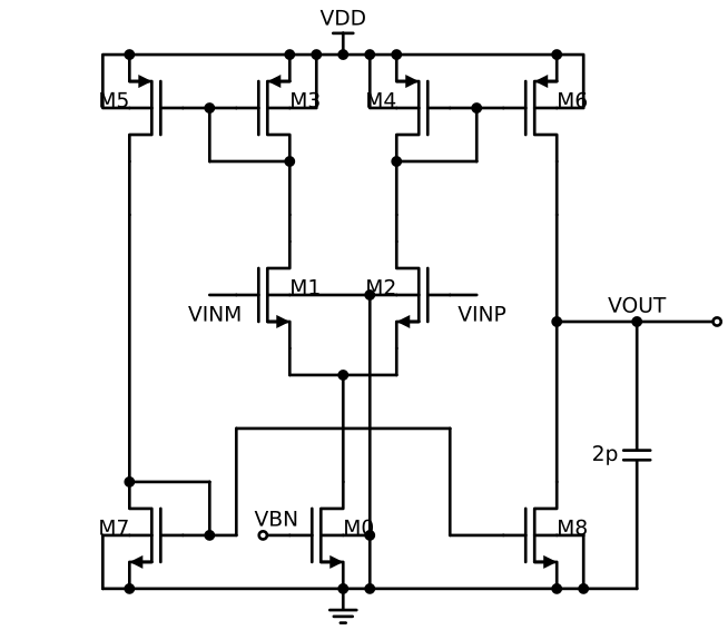
Round 5 — "Add a load capacitor"
Me:
Connect a capacitive load, , to the output — between and .
The capacitor drops from the output line to the rail, which was extended to meet it. The netlist line is CL VOUT 0 2p — LTspice rejects the c=2p form, so the value is written bare.
Adding it moved the input labels. The capacitor is drawn downward, which leaves schemdraw's drawing cursor pointing at , and the VINM/VINP labels added afterwards inherited that direction, so their offsets rotated and they landed on the gate leads. This is the same cursor-direction leak that turned the first folded cascode upside down. The fix is the same too: give the labels an explicit theta(0).
Round 6 — "Label it CL"
Me:
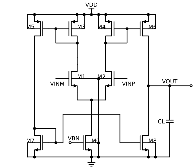
Change the capacitor's label from 2p to CL.
The visible label and the hidden one swapped places: CL is shown, and 2p rides along in an invisible label that only the converter reads. The netlist did not change.
Round 7 — "Route the mirror gate like ㄱ_"
Me:
For the gate connection, would it not be simpler to route it as ㄱ_ ?
ㄱ is the Korean letter shaped like a right angle turning down; ㄱ_ describes a line that runs across, drops, and steps sideways into a gate.
It was simpler. Until now the drawing had two separate verticals on the left: 's diode link at , and the bus climbing over at . Extending the diode link itself up over merges them; on the right the bus drops at and steps into 's gate. One vertical fewer, left and right now symmetric at , and the stray vertical beside the VBN label is gone. The netlist and the crossing count are unchanged.
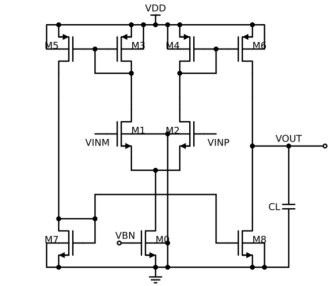
The final netlist, as extracted by LTspice itself:
M0 N003 VBN  0    0   NMOSA w=20u l=1u
M1 N001 VINM N003 0   NMOSA w=20u l=1u
M2 N002 VINP N003 0   NMOSA w=20u l=1u
M3 N001 N001 VDD  VDD PMOSA w=10u l=1u
M5 N004 N001 VDD  VDD PMOSA w=30u l=1u
M7 N004 N004 0    0   NMOSA w=10u l=1u
M4 N002 N002 VDD  VDD PMOSA w=10u l=1u
M6 VOUT N002 VDD  VDD PMOSA w=30u l=1u
M8 VOUT N004 0    0   NMOSA w=10u l=1u
CL VOUT 0 2p
Follow-up — "Does that bus touch the tail's drain?"
Me:
Routed that way, could the bus end up overlapping 's drain? Checking in LTspice should settle it.
LTspice connects two wires only where one wire's end lands on the other. Wires that merely pass through each other are not connected. So the question splits in two: does any wire end at the crossing points, and did LTspice keep the nodes apart?
In the generated .asc file, each of the three crossings has two wires passing through it and none ending there:
- drain lead mirror gate bus, at
- input pair bulk mirror gate bus, at
- input pair bulk tail arm, at
And in the netlist, 's drain is N003 (shared only with the input pair's sources) while the mirror gates are N004. Separate nodes, no short.
Me:
Then all we need to check is whether the wire sits at the same height as 's drain node, or dips below it into the device's territory. Let us make a rule: wiring must not intrude on a device's or a library block's boundary.
That reframing is better than the one I had. The geometric hazard is not the crossing itself but its height. A wire crossing a device's column exactly at a pin's height puts the pin on the wire, and LTspice connects it. A wire crossing lower than that runs through the device body. Above the drain pin is the only safe place to cross an NMOS; the bus crosses at against a drain at .
The rule went into the drawing practices:
- A device's body box spans from its gate terminal to its pin column, and from its source pin to its drain pin. A compound's box covers all of its devices and internal wiring. Outside wires may touch it only at its anchors.
- To cross a column, a wire must sit strictly outside the box and never at a pin's height. The one exception is a supply rail running through a source pin, which is an intended connection and must carry a junction dot.
A rule nobody checks drifts, so it also went into the checker, which now reports INTRUDE (a wire through a body box) and PIN-ON-WIRE (a pin in the middle of a wire with no dot). To see whether it actually catches anything, the bus height was deliberately broken:
- , as drawn: clean
-
, the drain pin's height:
PIN-ON-WIRE M0.drain (0, 24) -
, inside 's body:
INTRUDE M0 (-30,18)->(0,18)
The first version of the checker got the middle row wrong — it reported clean. A schemdraw Line is stored as a three-point path that includes its own midpoint, and the bus's midpoint happened to sit exactly on 's drain pin. Checked segment by segment, the pin looked like the end of a segment rather than the middle of a wire. The check now works on whole paths. Without the deliberate failure test, that gap would have shipped behind a clean OK.
What I am taking from this
A picture can be right while the circuit is wrong. Round 3 is the cleanest example I have seen: a correct schematic, produced by the same program that produced an incorrect netlist, because the renderer and the converter read two different copies of the same geometry. Extracting the netlist is not an optional final step. It is the only check on what the circuit actually is.
Some errors no tool will catch. The swapped input labels passed every automated check, because every check verified that the drawing was self-consistent, and it was. Polarity is a question about what the circuit does, and it took someone tracing the signal.
Ruling something out is not the same as trying it. The mirror compounds were rejected on a reading of their source. Actually using them surfaced a converter bug that affects every reversed compound, and that bug would otherwise have waited for some future circuit. The one real limitation, per-device sizing, was a few lines of code.
A checker earns trust by failing on purpose. The last post ended on this, and this session repeated it: the boundary check passed the real drawing on its first run and would have passed a broken one too. Breaking the input deliberately is what exposed it.
References
- Drawing a Folded-Cascode OTA in Three Rounds of Conversation — the previous circuit, and the junction checker this post extends
- An Old Engineer's Patience, and an AI That Finally Kept Up With It — the schemdraw-to-LTspice pipeline both posts build on
- schemdraw documentation
- Operational transconductance amplifier — Wikipedia
- Current mirror — Wikipedia
- LTspice — Wikipedia
Disclaimer: This blog post was created with assistance from Claude, an AI developed by Anthropic, under my direct supervision and guidance to ensure accuracy and alignment with my vision for the content.