Posted on September 27, 2026
Category: Technology
Tags: analog-ic-design, cmos, symmetrical-ota, ota, sky130, ngspice, gm-id, transistor-sizing, pvt-corners, monte-carlo, offset, python, ai-agents, circuit-design
Views: 10
Sizing a Symmetrical OTA on SKY130 in Ten Rounds of Conversation
In Drawing a Symmetrical OTA in Seven Rounds of Conversation the circuit was only a picture: schemdraw code, an LTspice netlist, and placeholder device sizes. This post picks up that schematic and sizes it for real, on the SkyWater SKY130 open PDK, simulated with ngspice.
As before, I am keeping the requests in the order I made them, including the ones where the answer was "that cannot be done." The design ended up where it did because of those.
The circuit and the spec
The topology is unchanged from the drawing: NMOS input pair with tail , diode loads , PMOS mirrors , and a 1:1 NMOS mirror that folds the left branch back to the output. One device was added: a diode-connected that takes the reference current and biases the tail through a 1:1 mirror.
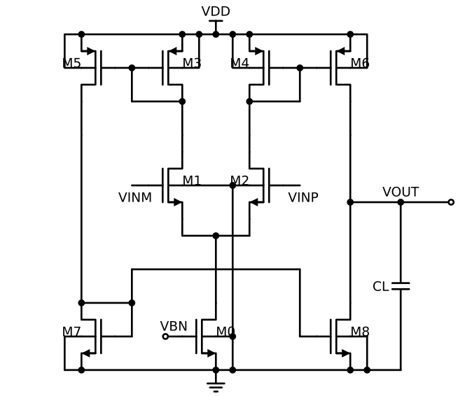
The specification I gave:
- , , ,
- Unity-gain frequency above , DC gain above , phase margin above
- must be scaled by a power of two (, …), and the smallest one that meets the UGF
- Every current mirror ratio is set with the m-factor, never by scaling
- Every device in the output branch stays saturated with the output within of either rail
- The final goal: meet all of that with the least current
Round 1 — "Design it"
Me:
We drew the symmetrical OTA in the schdraw project. Here, let us size it. Use ngspice or LTspice, and the SKY130 process — check whether the PDK is already on disk, and download the models if not. This is a simple circuit; your circuit knowledge should be enough.
The PDK was already installed through volare, so ngspice could load sky130.lib.spice directly. Before touching a simulator, Claude did the arithmetic that decides the current.
The single-stage OTA's unity-gain frequency is set by the input pair's transconductance, multiplied by the mirror ratio:
With , each input device carries and would need . That is past the weak-inversion ceiling of roughly –, so is out and is the first candidate (). The total supply current is then fixed by the topology:
The first simulation met UGF and phase margin but not gain (), and at the output PMOS fell out of saturation: against . Longer, wider output devices fixed both. A small sweep settled on and PMOS , giving , and at .
The claim that cannot work was also checked by brute force: an input pair of reached and a UGF of only .
A short aside followed. In the report I had called the "output stage," and the reply was:
What is this two-stage output? You are not designing a two-stage amplifier, are you?
No. It meant the output branch of the single-stage OTA. A small wording slip, but in analog design "output stage" names a whole architecture.
Round 2 — "Bound the gm/Id"
Me:
Use at most about 24 for the input pair's , and keep every other device below 20.
The existing design already complied — for the pair, at most elsewhere — so nothing changed except the harness, which now flags any device over its limit. The new bound did make the case even more clearly impossible: it needs 31.
Round 3 — "How did you pick the lengths?"
Me:
How did you decide the default channel lengths?
The honest answer: mostly by habit. The tail at and the input pair at were rules of thumb. Only two groups had actually been swept — the NMOS mirror (gain) and the PMOS mirrors (phase margin) — and even those on a coarse grid. There was no table behind any of it.
Round 4 — "Build the table, then minimise size across the worst case"
Me:
Make a table and choose the lengths again. Use lengths in multiples of , at least two units. Shrink the devices as far as the spec allows — and the spec includes the worst case.
(I first asked for multiples of and changed my mind mid-run.)
The characterisation swept for both device types at nine lengths from to . Two rows tell most of the story:
| () | 0.4 | 0.6 | 1.0 | 2.0 | 3.0 | 4.0 |
|---|---|---|---|---|---|---|
| nfet at | 108 | 191 | 172 | 202 | 258 | 303 |
| pfet at | 86 | 196 | 459 | 766 | 1275 | 1798 |
The NMOS intrinsic gain barely moves between and , while the PMOS gain climbs steadily. Since the output resistance is , the DC gain in terms is
where is each device's — and the NMOS term is the bottleneck.
"Worst case" was defined as five process corners (tt, ss, ff, sf, fs), three temperatures (, , ) and : 45 conditions, with the input common mode at . Each corner runs as one ngspice process that loops over temperature and supply internally, so all 45 conditions take under five seconds on 16 cores. A greedy optimiser then tries, for each device group, shortening (with and without keeping ) or narrowing by 15 %, and keeps the smallest candidate that still passes all 45.
The starting point — the Round 1 design — already passed, but thinly: worst-case UGF at fs//, and only of saturation margin on the tail.
Round 5 — "Plot the AC response"
Me:
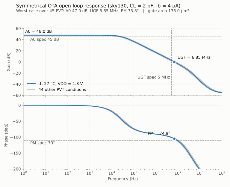
Save the AC result as a PNG plot too.
Every plot in this project shows the nominal condition as a single bold line and the other 44 PVT conditions as thin grey lines behind it, so the spread is visible at a glance.
Round 6 — "Put a floor under the saturation margin"
The first optimisation run shrank the gate area from to and passed everything — with of saturation margin on and on . That is exactly what "smallest area that meets the spec" produces: every constraint pushed onto its edge.
Me:
Add a 20 mV floor on the saturation margin and run it again.
Before it ran:
20 mV is too small too. Make it 100.
This is where the constraints collided. At the swing limit the output device has , so a margin needs
and the table says an NMOS only gets there at — while Round 2 capped it below 20. At , is about – even at room temperature. Swing, margin and the cap cannot all hold, and the table showed that before a single simulation ran.
Me:
Make it 50 mV.
Fifty was feasible, barely. The first generous starting point failed phase margin () because the big mirrors loaded the mirror nodes; a grid over mirror sizes found gain and phase margin trading against each other with no combination passing both. The way out was the input pair: its drain capacitance sits on the same mirror nodes, and shortening it to bought the missing degrees. From there the optimiser reached , with worst-case gain .
Round 7 — "Area is not a spec; current is"
Me:
I never gave you an area spec. It is fine if the area grows to meet the other specs. Reducing current matters more than area.
That settled the priority order: worst-case specs first, current second, area last. It also clarified something about the result. With the topology fixed at and ruled out in Round 1, is already the floor. Area was only ever the tie-breaker.
It also exposed a side effect of optimising for area. The optimiser had shrunk the tail and its reference to . A short tail device has low output resistance, so the difference between and costs tail current — and with it UGF.
Round 8 — "Would 0.8 µm on the tail help?"
Me:
Growing the tail to about seems fine. Would that give more margin?
| Tail | Worst UGF | margin | Worst | Area () |
|---|---|---|---|---|
| 1.2/0.4 | 5.30 MHz | 51 mV | 45.03 dB | 148.6 |
| 2.4/0.8 | 5.50 MHz | 51 mV | 45.07 dB | 151.4 |
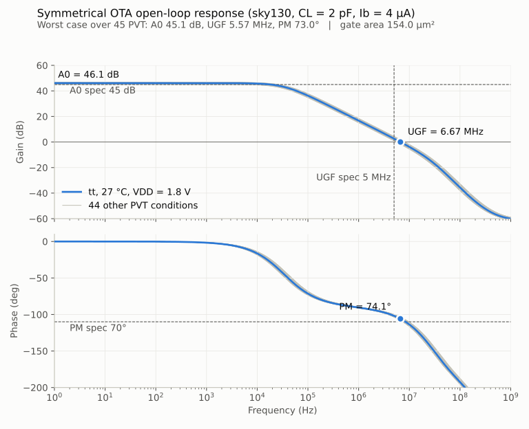
| 4.0/0.8 | 5.57 MHz | 67 mV | 45.08 dB | 154.0 |
It helped UGF and the tail's own margin, and did nothing for gain — which is set at the output node, not the tail. went in.
Round 9 — "Check the transient and the input common-mode range"
Me:
Check the transient response and the input common-mode range too. Save the plots as PNGs.
For the common-mode range, the output was held at by the same servo used everywhere else, and the input common mode swept from rail to rail while watching the smallest among –.
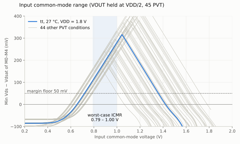
The lower limit is set by the tail , the upper by the input pair, whose drains sit at and therefore move with the supply. With a margin the worst-case range is –. At , a common mode of is only inside it.
For the transient, the OTA was connected as a unity-gain buffer and driven with steps that stay inside that worst-case range.
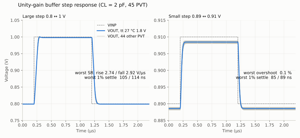
Worst-case overshoot is on the large step and on the small one, consistent with a phase margin. The measured slew rate, about , is below the textbook ; a step probably spends part of its 20–80 % window in linear settling rather than pure slewing, but I did not verify that. The first slew numbers came out in suspicious steps — , , — which was the sample grid showing through; interpolating the threshold crossings fixed it.
Round 10 — "And offset, by Monte Carlo"
Me:
Check the offset with Monte Carlo.
SKY130 exposes mismatch through *_mm library sections. The offset was defined as the differential input needed to put the output at , which keeps the buffer's finite-gain error out of the number.
Reading the model source first turned up a bug in my own netlists. The mismatch terms scale as
where mult is a subcircuit parameter that defaults to 1. The netlists passed only the SPICE multiplier m=2. The simulation was electrically correct, but every m-factor device would have received too much mismatch. Nothing in any plot so far would have shown it. The fix was to pass both, mult=2 m=2.
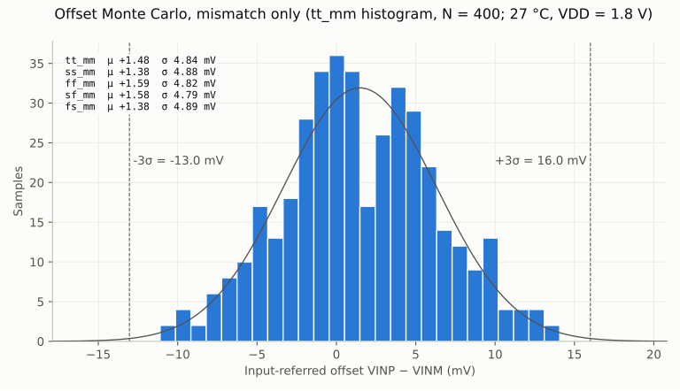
The result was , almost twice my hand estimate. The model explained why: besides the threshold coefficient ( for the nfet) there is a subthreshold-offset term of , and in weak inversion it moves the current just like does. The effective coefficient becomes
and with that the per-pair contributions add up to the simulated number: about from the input pair, from each PMOS mirror, and from the NMOS mirror. Running every device at high to save current is what makes this term matter.
Me:
Under 5 mV is enough for now — sigma, not three sigma.
It passes, with about to spare.
The final design
| Device | () | m |
|---|---|---|
| , | 4.0/0.8 | 1, 1 |
| , | 6.4/0.6 | 2 |
| , | 9.0/0.8 | 1 |
| , | 9.0/0.8 | 2 |
| , | 15.9/2.8 | 1 |
Ib vdd vbn 4e-06
CL vout 0 2e-12
XMB vbn vbn vss vss sky130_fd_pr__nfet_01v8 w=4.0 l=0.8 mult=1 m=1
XM0 tail vbn vss vss sky130_fd_pr__nfet_01v8 w=4.0 l=0.8 mult=1 m=1
XM1 x1 vinm tail vss sky130_fd_pr__nfet_01v8 w=6.4 l=0.6 mult=2 m=2
XM2 x2 vinp tail vss sky130_fd_pr__nfet_01v8 w=6.4 l=0.6 mult=2 m=2
XM3 x1 x1 vdd vdd sky130_fd_pr__pfet_01v8 w=9.0 l=0.8 mult=1 m=1
XM4 x2 x2 vdd vdd sky130_fd_pr__pfet_01v8 w=9.0 l=0.8 mult=1 m=1
XM5 y x1 vdd vdd sky130_fd_pr__pfet_01v8 w=9.0 l=0.8 mult=2 m=2
XM6 vout x2 vdd vdd sky130_fd_pr__pfet_01v8 w=9.0 l=0.8 mult=2 m=2
XM7 y y vss vss sky130_fd_pr__nfet_01v8 w=15.9 l=2.8 mult=1 m=1
XM8 vout y vss vss sky130_fd_pr__nfet_01v8 w=15.9 l=2.8 mult=1 m=1
| Item | Spec | Nominal | Worst of 45 PVT |
|---|---|---|---|
| DC gain | 46.1 dB | 45.1 dB | |
| Unity-gain frequency | 6.67 MHz | 5.57 MHz | |
| Phase margin | 74.1° | 73.0° | |
| Saturation margin | — | 51 mV | |
| Offset | 4.84 mV | 4.89 mV | |
| Supply current | minimum | 16 µA | — |
The DC-gain margin is a tenth of a decibel. At , with a saturation floor, DC gain and phase margin leave almost no room between them, and more area does not create any. The only lever left is current.
Afterwards — why is the NMOS mirror so long?
A later session went back over the design. The first question was about one number in the final table.
Me:
have , far longer than the other NMOS devices such as the tail. Was there a specific reason? I usually give the tail and the mirrors the same length, which also makes them easier to match in layout.
There was a reason, and it is the gain spec. The DC gain of this OTA is
sits on the output node, so its length goes straight into . The tail does not. Its output resistance affects common-mode rejection and tail-current accuracy but not the differential gain, which is why lengthening it from to in Round 8 moved by only . With a worst-case gain of against a spec, the optimiser could not shorten any further. They take of the total.
The width follows from the length. At the bottom of the swing has and needs of margin, so a long device has to be wide to keep down. Its worst-case margin is , on the edge as well. Pushing the length further runs into phase margin: a bigger loads the mirror node, and in Round 6 every combination with had a phase margin below .
Me:
Couldn't you lengthen the PMOS mirror a little, shorten , and balance the two? Or even use nearly the same length for both?
Claude's first estimate assumed for both devices. The Round 4 table says that is wrong for the nfet: its intrinsic gain is almost flat from to , while the pfet's rises steadily.
| () | 0.6 | 0.8 | 1.0 | 1.6 | 2.0 | 3.0 |
|---|---|---|---|---|---|---|
| nfet | 191 | 183 | 172 | 195 | 202 | 258 |
| pfet | 212 | 372 | 503 | 717 | 824 | 1342 |
| 1.1 | 2.0 | 2.9 | 3.7 | 4.1 | 5.2 |
Both at , tt, , . At equal current and the two devices have the same , so the ratio of intrinsic gains is the ratio of output conductances. Above the pfet's is two to six times smaller, and the NMOS mirror dominates the output conductance.
With the gain budget normalised to , the current design spends
and any pair of lengths that stays under that keeps . Rough numbers from the table, holding fixed to keep :
- Equal lengths. About for both would hold the gain, but the six PMOS fingers grow with . The mirror area goes from about to , and the capacitance on the node, which already sets the lowest non-dominant pole, roughly quadruples. That is worse on area and very likely fails phase margin.
- A partial balance. PMOS at with the NMOS mirror at about could save about , under 10 % of the total. The cost is about the capacitance on the node, against a phase margin with to spare.
The greedy optimiser could never have found the second option. It only shrinks devices, so trading length from one group to another was outside its moves. I decided a single-digit percentage was not worth a sweep for now, and none of these estimates were simulated. They come from a single tt point. But the reason for the long NMOS mirror in this PDK is now clear: it carries the gain, and in SKY130 its length buys gain far less efficiently than the PMOS's does. Matching it to the tail length for layout would cost gain or area here.
Afterwards — how the gm/Id table was built
The second question was about the method rather than the result.
Me:
The approach is very close to how I design, and I have met almost nobody else who works this way. Outside papers — mostly European ones — even textbooks barely explain it. Where did you pick it up?
Claude could not point to a single source: it learned from published literature, not from one book it remembers reading. The lineage itself is clear, though, and it is European. The method starts with Silveira, Flandre and Jespers at UCLouvain in 1996, and the EKV model from EPFL describes the same idea in terms of an inversion coefficient. It was later collected in Jespers' The gm/ID Methodology and in Jespers and Murmann's Systematic Design of Analog CMOS Circuits, whose companion lookup-table scripts spread it further. The standard textbooks still teach square-law sizing.
That matters here. Every device in this OTA sits between and , in moderate inversion, where the square law is simply wrong. A characterised table is the natural tool in that region.
Me:
To build the table I have always used a diode-connected device. How did you build yours?
Not with a diode. sim/charz.py holds the drain at a fixed voltage and sweeps the gate:
Vd  d  0  ±0.9        * |VDS| = 0.9 V, about VDD/2
Vg  g  0  0 -> 1.8 V   * DC sweep, 5 mV step
X_i d g 0 0  fet  W=4 L=L_i   * nine lengths, 0.4 to 4.0 um, in parallel
The bench runs at tt and with . It saves , , , and at each point, then interpolates to target values from 10 to 24. drops out only at the end, as .
| Diode-connected (sweep ) | Fixed (sweep ) | |
|---|---|---|
| Saturation | Guaranteed by construction, | Holds over the range used; must be filtered if swept wide |
| Independent variable | Current, easy to space logarithmically | Voltage |
| and | Taken at , like a mirror reference (, , ) | Taken at a chosen , closer to output devices (, ) and the input pair |
Me:
Isn't the diode better, though? It lets you assume the device is always saturated, and means nothing outside saturation.
Half of that holds. The diode does guarantee saturation, in weak inversion as well, since of a few hundred millivolts is far above the few that saturation needs. The fixed- bench is saturated too wherever it was used. Across to the table's never exceeds about , against . It only enters triode once the overdrive passes , at a far below anything in this design. A wider sweep would need a filter.
The other half, that means nothing outside saturation, is right. What neither bench can promise is saturation in the circuit. A table built in saturation says nothing about at the bottom of the swing, where its is . That is why the 45-corner harness checks on every device, whichever way the table was made.
In saturation, , and come out nearly the same from both benches, because the drain current depends only weakly on . They differ in the -dependent quantities, and . The real choice is where to read the intrinsic gain: at a mirror reference's , or at an output device's .
This table has two known gaps.
- It has a single , so at is not represented.
- It uses , while the input pair's sources sit on the tail node at about , so the body effect is missing.
The thorough version sweeps , , and together, as Murmann's scripts do. Here the table was only the starting point for the first sizing. The final word always came from the full 45-corner simulation.
What I am taking from this
Some specs are contradictions, and a table can prove it. The margin did not fail in simulation — it failed on paper, in one line: against a cap that keeps above . Characterising the devices first turned a long optimisation run into a two-minute conversation.
An optimiser does exactly what it is told. "Smallest area that meets the spec" produced margins, then a tail device short enough to cost UGF. Neither violated the objective. Both violated what I actually wanted, which was written down only after I saw the results: margins are part of the spec, and area ranks below current.
The most dangerous bug is the one that changes no picture. m=2 without mult=2 simulated a perfectly working circuit with the wrong statistics. It was found by reading the model source before trusting the Monte Carlo, not by looking at any output. The previous post ended on a schematic that was right while its netlist was wrong; this one has a netlist that was right while its mismatch was wrong.
"How did you choose that?" is worth asking. The first design passed, and its lengths were still guesses. Asking why is what led to the table, the worst-case run, and everything after.
References
- Drawing a Symmetrical OTA in Seven Rounds of Conversation — the schematic this post sizes
- SkyWater SKY130 PDK documentation
- volare — open PDK version manager
- ngspice — open source spice simulator
- A gm/ID based methodology for the design of CMOS analog circuits — Silveira, Flandre, Jespers, IEEE JSSC 1996
- Systematic Design of Analog CMOS Circuits — Jespers, Murmann, Cambridge University Press 2017
- An analytical MOS transistor model valid in all regions of operation — Enz, Krummenacher, Vittoz, 1995 (EKV)
- The gm/ID Methodology, a sizing tool for low-voltage analog CMOS circuits — Jespers, Springer 2010
- Tradeoffs and Optimization in Analog CMOS Design — Binkley, Wiley 2008
- IIC-OSIC-TOOLS — open-source IC design environment from JKU, with gm/ID material for SKY130
- Operational transconductance amplifier — Wikipedia
- Current mirror — Wikipedia
- Monte Carlo method — Wikipedia
Disclaimer: This blog post was created with assistance from Claude, an AI developed by Anthropic, under my direct supervision and guidance to ensure accuracy and alignment with my vision for the content.