Posted on September 30, 2026
Category: Technology
Tags: analog-layout, cmos, ota, operational-transconductance-amplifier, sky130, skywater, open-source-pdk, klayout, python, pcell, drc, lvs, mim-capacitor, common-centroid, interdigitation, device-matching, ngspice, parasitic-extraction, post-layout-simulation, eda, ai-assisted-design, claude
Views: 8
"Laying Out a Symmetrical OTA on SKY130 with KLayout Python: A Conversation"
In the previous post I sized a symmetrical OTA on SkyWater SKY130 over ten rounds of conversation with Claude. This post picks up where that one stopped: turning the schematic into a DRC- and LVS-clean layout.
The ground rules I set at the start:
- Use KLayout as the layout tool, and drive every step from its built-in Python.
- Use the transistor PCells that come with the PDK.
- Do not use the ALIGN placer/router I had set up in another project. The circuit is small enough to place by hand.
- Lay out the input pair in an interdigitated style.
What follows is the session, lightly edited, with "Me" as the designer and "Claude" as the assistant.
The Circuit and the Sizing
The OTA has ten transistors plus a 2 pF load capacitor. The NMOS input pair M1/M2 sits on the tail transistor M0. The PMOS diode loads M3/M4 mirror their currents 1:2 into M5/M6, and the NMOS mirror M7/M8 folds the left branch onto the output. MB, drawn as a separate inset, turns the bias current into the tail gate voltage vbn. The blue labels are the internal net names used throughout the layout.
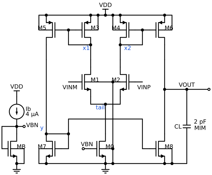
The final sizing from the previous post was:
| Device | Role | Total W (µm) | L (µm) |
|---|---|---|---|
| MB, M0 | Tail current mirror | 4.0 | 0.8 |
| M1, M2 | Input pair | 12.8 | 0.6 |
| M3, M4 | PMOS diode loads | 9.0 | 0.8 |
| M5, M6 | PMOS mirror outputs (1:2) | 18.0 | 0.8 |
| M7, M8 | NMOS output mirror | 15.9 | 2.8 |
Bias current is 4 µA and the supply is 1.8 V. The load was an ideal capacitor in the schematic; in the layout it becomes an on-chip MIM capacitor.
Round 1: Where Are the PCells?
Me: The PDK should be in my ALIGN project directory. Use its MOS PCells.
Claude: The ALIGN tree only has Magic technology files for SKY130 (SKY130.tech, .magicrc), with no KLayout PCells. The SKY130 install your simulations used is the volare-managed build of sky130A, and that one does ship KLayout PCells under libs.tech/klayout/pymacros. But loading them in KLayout 0.28.16 fails:
ModuleNotFoundError("No module named 'gdsfactory'")
Those PCells (originally from Mabrains) build geometry with gdsfactory and import gdsfactory.types, an API that only exists in gdsfactory 6.x. So even installing the current gdsfactory would not help.
Me: Search the web for a PCell set that works first. If nothing turns up, install gdsfactory 6.
Claude: Matthias Köfferlein, the author of KLayout, publishes sky130A_el: pure pya PCells with no external dependencies, plus DRC/LVS setup. Its MOSFET PCell supports multiple fingers and loads fine in 0.28.16. It has no MIM PCell, so I'll draw the capacitor directly on the capm layer.
The final tool mix was therefore:
- Transistor PCells:
sky130A_el(cloned intothird_party/, not committed) - DRC, LVS, and layer properties: the
sky130AKLayout decks from the volare install (open_pdks version1.0.466-0-gbdc9412) - SPICE models: the same volare
sky130Angspice library the sizing used
Round 2: A First Layout, and What DRC and LVS Found
The generator places each device as a row of two-finger units (source–gate–drain–gate–source), with dummies at the row ends. Each row has metal-2 gate tracks below the devices and metal-2 source/drain tracks above, and a metal-3 column per net ties the rows together.
The first DRC run with the PDK deck reported 310 violations, falling into three groups:
- Off-grid contacts (264). M7/M8 split into four fingers of . The PCell centers its contacts at , which lands on a 2.5 nm half-grid.
Claude: Rounding the finger to 3.98 µm keeps on the 5 nm grid. The total becomes 15.92 µm (+0.13%), identical for both M7 and M8, so the mirror ratio is untouched.
-
Implant spacing (
nsd.2,psd.2). Adjacent units left a 0.15 µm gap between their implant layers, below the 0.38 µm minimum. Covering each row with a single implant rectangle removed it. -
The remaining contact-size errors disappeared with the grid fix.
After that, DRC was clean, but LVS was not. The current-mirror gates came out as floating nets.
Claude: In the mirror rows, the gate net (y, vbn, x1, x2) is also one of the source/drain track names. I built the track list by merging two dictionaries, gy | ty, so the gate track was silently overwritten. Iterating both lists fixed it, and KLayout printed Congratulations! Netlists match.
This bug is invisible to DRC. It is a good reminder that a DRC-clean layout says nothing about connectivity.
Round 3: ABBA or ABAB?
Me: Change the interdigitation from D-A-B-B-A-D to D-A-B-A-B-D.
Claude made the change (DRC and LVS stayed clean), and then I asked the real question.
Me: From a matching standpoint, isn't ABAB better than ABBA?
Claude: With only two units per device, ABBA is better. Model a linear process gradient, such as a threshold-voltage tilt across the row, as
Then each device's effective threshold is the average over its unit positions. For ABBA, A sits at positions 0 and 3 while B sits at 1 and 2, so both centroids are at 1.5 and the term cancels. For ABAB, A's centroid is 1 and B's is 2, leaving a mismatch of
where is one unit pitch, 2.43 µm in the input pair. ABAB's advantages are elsewhere. Each device gets one edge unit, and its offset stays at one unit as the pattern grows, so the relative error shrinks with many repetitions. The dummies already handle the edges, and we don't have many repetitions.
Me: Then put it back to DABBAD.
Round 4: Keep Signals Off the Devices, Fill the Gaps, Split the MIM
Next I asked for three changes at once:
- No signal metal may pass over a transistor.
- Fill empty space with dummy devices.
- Split the 2 pF MIM into smaller units.
Claude moved every inter-row metal-3 column into side channels outside the device array, with symmetric nets in mirrored positions (x1 and x2, y and vout, vinm and vinp). A short KLayout script confirmed that metal 2, 3, and 4 have zero overlap with diffusion or poly. Narrow rows were padded with dummy units up to the width of the widest row.
Round 5: Where Should the Tail Mirror Go?
Me: The third row looks like it's MB/M0 for the tail current. Put it in the same row as M7/M8, to the left of M7/M8.
That worked, but it moved M7/M8 off the chip's symmetry axis.
Me: For symmetry, put MB/M0 between M7 and M8.
Claude: Putting all of M7 on the left and all of M8 on the right would separate their centroids by about 25 µm. Instead I split the M7/M8 ABBA in half and inserted MB/M0 in the middle: D M7 M8 | D MB M0 M0 MB D | M8 M7 D. Both pairs keep their centroids on the axis. The remaining flaw is that M8's inner units now face small tail dummies while M7's outer units face large ones.
Me: Or would it be better to keep M7/M8 in the center and split MB/M0, interdigitated, to the outside left and right?
Claude: Yes, and the reason is which mismatch hurts more. An M7/M8 mismatch unbalances the currents in y and vout, which appears directly as input-referred offset. An MB/M0 mismatch only shifts the tail current by a few percent, changing and UGF slightly. So M7/M8 deserve the best spot: contiguous, centered, with identical neighbors. MB/M0 can absorb the cost of being split wide. A split ABBA still cancels linear gradients, but second-order gradients leave an error that grows with the spread.
The final bottom row became:
D MB M0 | D M7 M8 M8 M7 D | M0 MB D
Round 6: Tightening Everything to DRC Minimums
Me: The MIM doesn't need to be m = 8. Choose m so it fills the width. And the devices seem far from the p-guard ring. Unless there's a reason, use the minimum spacing DRC allows.
For the capacitor, each unit is sized from the PDK's typical MIM densities, and :
The generator tries m = 1 to 12 in a single row spanning the guard ring's width, and picks the m whose unit is closest to square. It landed on m = 3 units of 18.84 × 17.33 µm, 666.7 fF each, 2000.2 fF in total.
For the guard ring, the side gap existed only because the routing channel sat between the devices and the ring. Moving the channel outside let the ring sit at the diff-to-tap minimum of 0.27 µm (difftap.3). The gap between the NMOS and PMOS rings had no reason either, so we swept it with DRC:
| Ring-to-ring center spacing (µm) | DRC result |
|---|---|
| 0.60 | difftap.3, m1.2 violations |
| 0.65 | difftap.3 violation |
| 0.68 | clean (0.41 µm tap + 0.27 µm spacing) |
| 0.70 | clean |
Me: Is the distance between the MIM and the p-guard ring really the DRC minimum? It still looks far.
Claude: No. There is no DRC rule between the MIM layers (metal 3, capm, metal 4) and the guard-ring layers (tap, metal 1). The 3 µm gap was room I had left for a via stack and the vout connection.
Me: Oh, right. The power rails are missing. Make VDD and VSS 5 µm wide, and keep the MIM away from VSS too.
That added 5 µm metal-1 rails outside each ring. The wide metal immediately tripped m1.3ab, the 0.28 µm spacing required next to metal wider than 3 µm, at small notches in the ring corners. Filling the corners fixed it. The MIM sits 1.2 µm below the VSS rail, a value borrowed from capm.2b since no rule dictates it, and its bottom plate reaches the rail through metal-3 tabs.
Me: The rails only overlap the middle of the guard ring's outer metal. Wouldn't it be cleaner to cover it completely?
It was, and it was a one-line change. The final layout is 66.9 × 61.2 µm, with zero DRC violations and a clean LVS.
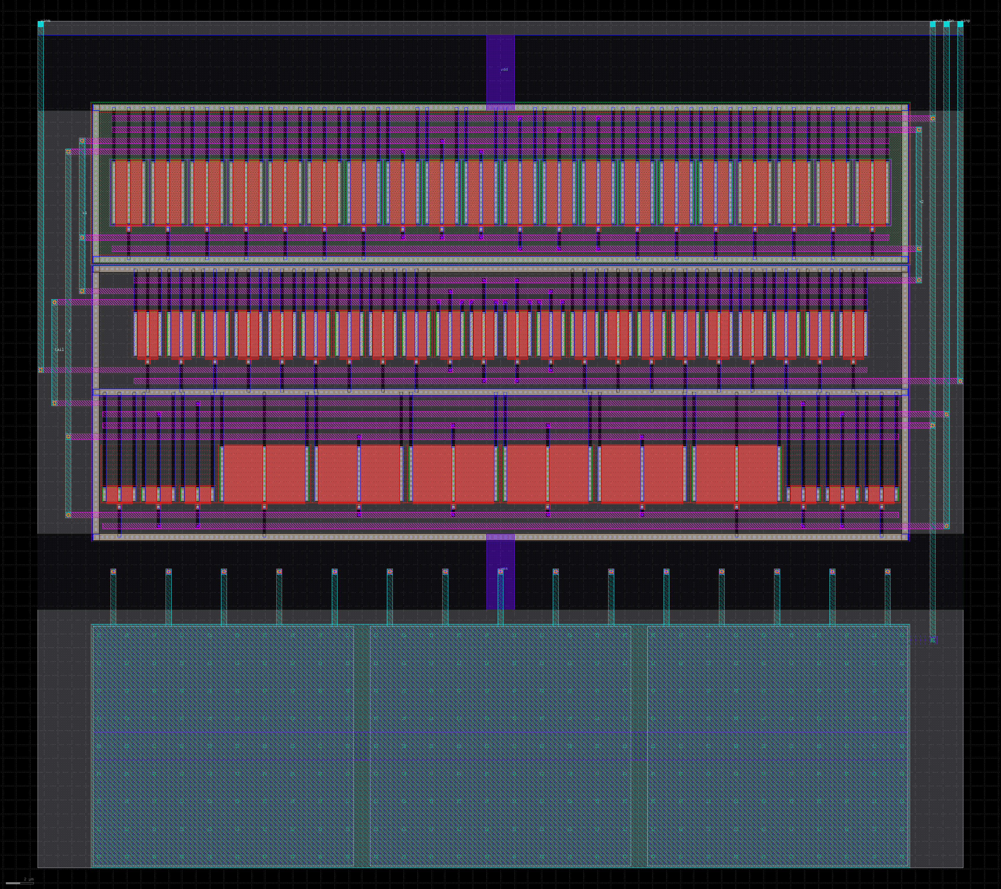
The video below replays the generator from the schematic to this final layout, in the order a layout engineer would draw it by hand (watch on YouTube).
Round 7: Does It Still Work After Extraction?
Me: Can the PDK do parasitic extraction? Run a typical-corner simulation to check that it works.
Claude: In this open PDK and toolset, analog parasitic extraction means Magic. The OpenRCX rules in the PDK target the digital OpenROAD flow, no Calibre or StarRC decks are included, and KLayout 0.28's extraction is device-level only.
We tried Magic. The Ubuntu package is Magic 8.3.105 from 2021, and the PDK techfile refused it:
Error:  Magic version 8.3.411 is required by this techfile,
but this version of magic is 8.3.105.
After that, Magic crashed with a segmentation fault. The PDK's sky130A.magicrc also hard-codes the path of the machine that built it (/Users/donn/...), so it needs a local copy with the path replaced. Building a newer Magic is left for next time.
Me: If KLayout's SPICE extraction works simply, try that first.
The netlist that the LVS deck extracts already contains each transistor's real layout geometry: source/drain junction areas and perimeters (AS, AD, PS, PD) and the MIM. Converting it to PDK subcircuit calls and running ngspice hit three traps:
- No compatibility mode. Without
set ngbehavior=hsain.spiceinit, the PDK models do not load. - Model binning. LVS merges fingers, so a dummy shows up as a single transistor with
W = 126 µm, beyond the model's single-finger bin range. BSIM4 bins by , so the converter passes the layout's finger count asnf. - The MIM multiplier. In the PDK's MIM model,
mfonly feeds the Monte Carlo term; it does not multiply the capacitance. One instance withmf=3gave 0.67 pF, and the UGF jumped to 16.6 MHz. The fix was to emit three separate instances.
Me: Estimate the wire capacitance too, and simulate with it.
A 75-line KLayout script rebuilds each net's connectivity through poly, li, and metal 1 to 4. It then multiplies each net's area and perimeter by the nominal substrate capacitances from the PDK's Magic techfile. Gate poly, diffusion, and the metal 4 above the MIM are excluded, since the device and MIM models already account for them. One subtlety: the vias on the MIM's top plate must not be connected to the metal-3 bottom plate, or the capacitor's two plates short together.
| Net | Wire C (fF) |
|---|---|
| x1, x2 | 20.1, 20.5 |
| y, vout | 27.7, 18.6 |
| tail, vbn | 17.6, 17.9 |
| vinp, vinm | 8.7, 8.4 |
The results at the typical corner (tt, 27 °C, 1.8 V):
| Metric | Schematic | Extracted | + Wire C |
|---|---|---|---|
| A0 (dB) | 45.35 | 45.35 | 45.35 |
| UGF (MHz) | 6.570 | 6.539 | 6.437 |
| PM (°) | 74.11 | 73.77 | 72.12 |
| IDD (µA) | 15.23 | 15.23 | 15.23 |
| Offset (mV) | 1.585 | 1.585 | 1.585 |
The OTA works. The extra capacitance on the mirror nodes (x1, x2, y) lowers their poles and costs about 2° of phase margin, while 18.6 fF on vout barely matters next to the 2 pF load. The estimate ignores coupling capacitance, shielding, and wire resistance, so a proper Magic extraction remains the next step.
What I Took Away
- A layout generator in plain Python is enough for a small analog block. The whole generator is about 350 lines, and every change in this post was an edit to a list or a constant, followed by a DRC and LVS rerun.
- Run DRC and LVS after every change. Two of the worst bugs, the overwritten gate track and the disconnected MIM top plate after a row got wider, were invisible to DRC and caught only by LVS.
- Matching is about priorities, not a single pattern. ABBA beat ABAB here, and which mirror got the center of the row mattered more than making everything look symmetric.
- "Minimum spacing" deserves a question. Several gaps turned out to be leftovers from earlier routing choices rather than rules.
- Open-PDK tooling has version cliffs. The PCells needed a gdsfactory version that no longer exists, and Magic needed a newer build than the OS provides.
References
- SkyWater SKY130 PDK (google/skywater-pdk)
- SkyWater SKY130 PDK documentation
- open_pdks: PDK installer that builds sky130A, including its KLayout and Magic setup
- volare: version manager used to install sky130A, build
bdc9412b(open_pdks 1.0.466) - sky130A_el: basic PCells, DRC, LVS for sky130A by Matthias Köfferlein
- sky130_klayout_pdk: Mabrains' gdsfactory-based PCells, the ones shipped in sky130A
- gdsfactory
- schemdraw: used to draw the schematic
- KLayout
- KLayout LVS documentation
- Magic VLSI layout tool
- ngspice
- ALIGN: Analog Layout, Intelligently Generated from Netlists
- Sizing a Symmetrical OTA on SKY130 in Ten Rounds of Conversation (previous post)
Disclaimer: This blog post was created with assistance from Claude, an AI developed by Anthropic, under my direct supervision and guidance to ensure accuracy and alignment with my vision for the content.