Posted on October 13, 2026
Category: Technology
Tags: analog-ic-design, cmos, symmetrical-ota, ota, sky130, ngspice, geometric-programming, convex-optimization, global-optimization, gm-id, ekv-model, transistor-sizing, pvt-corners, cvxpy, python, ai-agents, circuit-design
Views: 4
Global Optimization of a Symmetrical OTA on SKY130: Geometric Programming Across 45 PVT Corners
In Sizing a Symmetrical OTA on SKY130 in Ten Rounds of Conversation the OTA was sized the usual way: gm/Id tables, a greedy worst-case search, and a lot of simulation. The final hand design meets every spec at all 45 PVT conditions. It draws , uses of gate area, and the search behind it took 17,685 SPICE operating-point runs.
This post asks a different question: can the same circuit be sized by an optimizer that returns a global optimum, is that optimum better than the hand design, and how much faster is it to get there? The tool is geometric programming (GP). The work took four sessions, and most of it turned out not to be about the optimizer at all. As before, I am keeping my requests in the order I made them, compressed to the turning points.
The circuit and the spec
The circuit is unchanged: NMOS pair with tail biased from , diode loads , PMOS mirrors , and an NMOS mirror folding the left branch to the output.
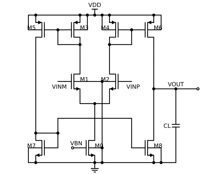
The spec is also unchanged, and it is tight:
- , , mirror ratio , tail mirror kept at
- , , , offset
- Every device saturated with , including the output devices with the output from either rail
- All of it at each of 45 PVT conditions: 5 process corners, 3 temperatures (, , ), 3 supplies (, , )
- Objective: least supply current first, then least area
Round 1 — "Rewrite every spec as a posynomial"
Me:
Last time the sizing relied on your circuit knowledge. This time let us research how to optimize it. Rewrite every OTA spec — gain, PM and so on — as posynomials that include each device's gm/Id, build an objective that minimizes the total device size, and solve it by geometric programming. Use the EKV (v2.6) equations where GP needs them. Can you do that?
And a little later:
Do you think EKV is the right choice here, or is there something better?
The ultimate goal is a general-purpose sizing method, one I can apply to other OTAs later.
What a geometric program is
A monomial is a function with and any real exponents. A posynomial is a sum of monomials. A geometric program is:
with every a posynomial and every a monomial, over positive variables . The point of the form is a change of variables. With , a monomial becomes the exponential of an affine function of , and the log of a posynomial becomes a log-sum-exp, which is convex. A GP is a convex problem in disguise. Every local optimum is the global optimum, an interior-point solver finds it in seconds without a starting point, and if the solver says "infeasible," then no design in the model meets the spec.
Hershenson, Boyd and Lee showed in 2001 that a two-stage op-amp can be written this way with square-law devices. Square law is the weak link: every device in this OTA runs in moderate inversion, at between 16 and 23, where square law is off by tens of percent. So the work splits in two. The circuit equations are easy. The device equations are where the accuracy lives.
The circuit equations
Most specs are posynomial almost as written. The gain of the symmetrical OTA and its unity-gain frequency become:
The offset from Pelgrom mismatch, with , is a posynomial in transconductance ratios:
The objective started as total area, but I changed the priority once I saw it at work: current first, then area, because spending current makes small devices easy. In the final form it is a single product . With it is pure minimum current; with , 1 % less current is worth 1 % more area.
The device equations: inversion coefficient and gm/Id
The gm/Id method sizes a transistor by choosing how strongly it is inverted rather than by choosing an overdrive voltage. The natural variable for that is the inversion coefficient from the EKV model:
is weak inversion, is strong inversion, and this design lives between about and . The definition is a monomial equality, so , , and of every device are GP variables tied together exactly.
EKV also gives as one expression valid in all regions:
It tends to in weak inversion and falls as in strong inversion. That was the answer to the question of whether EKV is the right choice: its structure is exactly what GP wants. Fitted to SKY130 tables as it stands, it was off by 11 % rms. One extra term, , standing in for velocity saturation and mobility reduction, brought the error to 1.9 %:
This is a valid GP constraint as written. A positive fractional power of a posynomial is still log-log convex, and CVXPY's disciplined GP accepts it directly. The parameters , and are fitted jointly per length, and each is then expressed as a monomial .
Much later I asked about the fitted value of :
You did not just use a constant like 1.4, did you? Isn't n usually below 1.5?
It was not a constant: it ranges from 1.5 to 1.9 for the nfet and is about 2.0 for the pfet, against a physical slope factor of 1.3 to 1.5 in BSIM. That is not a mistake, but it has to be read correctly. In a joint fit the parameters absorb the model's shape error, so they form a coordinate system rather than a measurement. The values in this post are on the fit's own scale.
Everything else: max-of-monomials fits
While the first fits were running, I checked the plan for whatever EKV could not cover:
Where EKV does not fit well, the plan is to fit the data and turn it into monomial or posynomial functions, piecewise or over the whole range, right?
That is what was done. The remaining quantities (, , capacitance per width) have no compact physical formula. They are fitted from ngspice tables as the maximum of a few monomials. This is the GP-compatible form of a convex piecewise-linear fit in log space:
These quantities sit on the "less than" side of each spec, so an upper fit keeps the GP conservative.
Round 2 — "Isn't GP supposed to be global?"
Two specs did not fit the pure form. The EKV constraint only bounds from above. That is fine where a spec wants large, but in the offset formula sits in a numerator, and the solver could report a smaller than physics allows. Phase margin is a sum of arctangents of pole ratios, and an arctangent is not a posynomial. Claude handled both with sequential GP (SGP): replace each awkward term by a monomial bound around a previous solution, solve, repeat. The cold start of that loop kept failing.
Me:
What is SGP, and why does the cold start fail? I thought GP gives a global optimum, with no dependence on the initial value.
With SGP, global optimality is no longer guaranteed, and I do not like the dependence on the initial value. What about two steps? If the device sizes can be found first from only the specs that GP can express, do that in phase 1. Then use the result as the initial condition of the SGP problem with all specs in phase 2.
That became the structure of every solve. Phase 1 is two pure GPs with opposite approximations, so each one is a true global optimum of its own problem:
- relax drops or loosens the non-GP terms ( in a numerator is left as the free variable, the arctangent is bounded by a chord). Its optimum is a lower bound on the true optimum.
- safe replaces them with conservative monomials: the denominator by its AM-GM lower bound, the arctangent by its tangent at zero. Its optimum is a guaranteed feasible design.
Phase 2 is SGP started from the safe solution. Each step tightens the AM-GM and tangent bounds around the previous point, so every step stays feasible and is no worse than the last. The true optimum is bracketed between relax and the SGP result.
I pushed on what that means:
If GP is solvable in a given design space and returns a result, isn't that the optimized result? Shouldn't the answer be a yes or a no?
For the pure GPs it is a yes or a no. SGP adds refinement. In practice the safe point was within 1 % of the converged optimum, and two SGP steps matched full convergence to four digits in 52 s instead of 144 s.
So SGP is a kind of fine tuning.
That is the right way to see it. The honest claim is a global optimum of a convex inner approximation, plus a fine-tuning step whose gap is measured.
Round 3 — "Put every corner into one design space"
The first GP was sized at tt, , with targets set to the hand design's tt performance. It came back at and , smaller than the hand design, and failed the 45-condition SPICE check on saturation at the swing ends: 14 to 36 mV of margin against 50. The hand design passes.
My first idea was design centering by overspec:
We already have equations for every spec. Put the tt GP sizes and the fitted corner parameters into them, and we can predict how far each spec will drift at the worst case. Then solve the tt GP again with that much overspec.
It failed for a structural reason. The drift between tt and the worst corner depends on the design, so the drift measured on one design is wrong for the next one, and the second solve became infeasible. So I changed the approach:
Let us rethink this. Instead of two GP solves, do one, and widen the design space so it contains the corners. Put the multi-corner GP into a single design space and solve it once. If each corner's design space is 1×1, do not run a GP in each one; run one GP over the 3×3 space that contains them all.
The spec stays the same everywhere. What changes per corner are the constants inside the GP constraints.
In GP form this is natural. Every condition gets its own copy of the device equations, built from that condition's fitted model. Widths, lengths and currents are shared, while , , and are per condition. The feasible set is the intersection of all 45, so a solution meets every condition at once. It takes 15 model files (5 corners × 3 temperatures). The supply only enters the headroom equations, so it stays a constant in the formulas.
Earlier I had worried that more variables would make the optimum harder to judge. It does not. The design variables do not grow with the number of conditions. Only the per-condition state variables do, and they are fixed by the design variables. The problem stays convex.
Round 4 — "L belongs in the design space too"
The first multi-corner version still treated lengths as a discrete grid and solved one GP per combination of and the group lengths, 2,662 of them in the last version. While watching it run, I stopped it:
Going about it this way does not seem to mean much.
Put the L enumeration into the design space as an equation. If it is in the design space, one GP solve per B should be the end of it.
That required fitting each device quantity as a function of , and that is where the first real modeling problem appeared. In SKY130, nfet rises with up to about , stays flat to , and then falls steeply. In log-log space that is a hump, a concave shape. A max-of-monomials fit is convex, so it cannot follow a hump. Its rms error floors around 10 % no matter how many monomials are used.
The optimizer then did exactly what an optimizer does. It went to the lengths where the fit was most optimistic, to on the NMOS mirror, and the SPICE gain came out 0.6 dB below the model's prediction.
Can't we express two pieces as a piecewise-linear equation and put them into one space? Or split it in two and double the design space?
Doubling the space does not work the way corners do. Corners must all hold, an intersection, which a single convex problem handles. Length segments are alternatives, a union, and the choice between them sits outside convexity. But the hump's corners line up with the BSIM length bins at and . Split there, each of the three segments is convex on its own. The GP assumes a segment per device group, solves, checks where each length landed, and re-solves with those segments until nothing moves:
Let us try the concave upper-bound iteration.
It converges in about two passes. A six-condition solve went from 1,434 s with enumeration to 13 s. The full 45-condition solve takes about two minutes per value of .
Round 5 — "Manual passes with B = 2"
After every GP solution, the pipeline runs the 45-condition SPICE check and feeds the shortfalls back as per-condition targets for the next solve. The aim was the hand design's , which halves the input-pair current needed for a given UGF. Instead, kept dropping out and the loop fell back to .
Several model fixes went in along the way. The fit was weighted 10× in the operating window, which brought the model's average gain bias from to . The fit gained and axes, because it had ignored body effect on the pair and the low at the swing ends, together worth up to 4 mV at . Then I looked at the correction loop itself:
Does the correction adjust every spec at once, or only raise the ones that fell short?
Isn't adjusting all of them at once the problem? Only the specs that fell short should move.
It had been resetting every target at every condition on every round, so it raised targets that already passed. Changed to ratchet up only on shortfalls, it finally passed:
| Version | Change | Round 0 () | Outcome |
|---|---|---|---|
| v1 | 45-PVT single GP | A0 44.62 dB, FAIL | B = 2 dropped in round 1; B = 1 NEAR |
| v3 | fit weighted in the operating window | A0 44.94, sat 47.7 mV, FAIL | B = 2 dropped again |
| v4 | fit with and axes | B = 2 infeasible in the GP | B = 1, A0 stuck at 44.89 |
| v5 | correction raises shortfalls only | — | B = 1 PASS: , |
That is 35 % more current and 71 % more area than the hand design.
The manual design was done with B = 2 and passed every corner, so the spec is not impossible.
So "B = 2 is infeasible" was not a statement about the circuit. It was a statement about the model, or about the design space.
Round 6 — "Why does the GP solution fail in SPICE?"
Me:
Compare with the manual sizing for now. The biggest problem is finding out why the GP solution, especially with B = 2, does not meet the spec in SPICE, and fixing it.
Claude wrote a script to evaluate any fixed design with the GP model at its SPICE operating points, condition by condition, and ran it on the hand design. Up to then every model bias had been measured on the optimizer's own solutions, and that is a blind spot. If the model is pessimistic in some region, the optimizer avoids that region, so the bias never shows up in the solutions being checked.
On the hand design, the model's gain was 1.1 to 1.66 dB too low at all 45 conditions. Split by term, was overestimated by 12 to 18 % and by 7 to 10 %.
The NMOS mirror explained most of it. The hand design draws as one finger of . The GP's design space allowed fingers up to , and its models were characterized at . A single-device simulation with the same total width, length, current and separated the effects:
- one finger against eight fingers: ratio 0.85 to 0.86
- the model against the eight narrow fingers: 0.98 to 0.99
The model was accurate for the device it described. The device it described was not the one in the hand design. BSIM parameters are binned in width as well as length, and a sweep of finger width shows the steps:
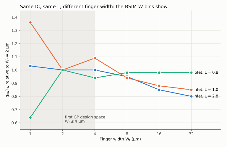
The steps are not monotonic, so a smooth monomial correction such as cannot model them. Instead, finger width became a discrete choice per device group, with a full model set at each bin: , , and , 60 model files in all, solved in parallel. The pfet fit, which had been 7 % pessimistic at the fast-slow corner only, was split at the length bins like the nfet's. Re-evaluated, the hand design's gain bias at the binding condition went from to .
So in the end, the GP solver did not fail because the spec was hard to reach. The problem was the accuracy of the model the GP used?
Then it sounds like with the GP solver would still find no solution.
Both, and the second one was checked in SPICE. The new GP's solution uses a single finger on the NMOS mirror. Redrawn as with the same total width, it fails at . With fingers capped at , really is impossible under this spec. The earlier "infeasible" answers were correct for the space the optimizer was given; that space just did not contain the hand design.
The correction loop showed one more failure along the way. Raising each target by exactly its shortfall shrinks the shortfall geometrically, so it approaches the spec boundary and never crosses it. In the end the remaining shortfall was smaller than the 0.01 µm rounding of a finger width, and the design stopped changing at 49.98 mV of margin. A small guard band (0.5 mV on saturation, 0.5 % on UGF) fixed it, and passed in round 2.
Round 7 — "Why is the pfet Vdsat optimistic?"
One bias remained. At the swing end, the fit was about 3 mV optimistic for the output PMOS. A one-at-a-time decomposition (real against characterization , real against reference width, real against grid length) left almost all of it as pure fit error. Two things bent the fit:
- points near the linear region (, about ), which the circuit never uses
- the kink at the length bin
Filtering the table to and , and splitting at the same length bins, cut the worst error in the operating window from to .
With that model, the pipeline passed all 45 conditions on the first GP solution, with no correction rounds: 138 SPICE runs and 170 s in total.
Round 8 — "Run it once more with a larger area weight"
Me:
Set w-area to 1.0, run the GP pipeline once more with B = 2, and compare again, including the manual design's IDD.
With the first two solutions missed the offset spec by a fraction of a millivolt (5.04 and 4.98 mV in Monte Carlo, against 4.84). The offset correction fixed it in round 2.
The result
All three designs were measured on the same bench: 45-PVT worst case for every spec, supply current at tt, and offset from a 200-run mismatch Monte Carlo.
| Spec | Manual | GP, | GP, | |
|---|---|---|---|---|
| / () | — | 4.000 / 15.39 | 3.511 / 13.67 (−11.2 %) | 3.699 / 14.20 (−7.7 %) |
| Area () | — | 154.0 | 177.9 (+15.5 %) | 153.0 (−0.6 %) |
| (dB) | ≥ 45 | 45.08 | 45.04 | 45.05 |
| UGF (MHz) | ≥ 5 | 5.573 | 5.060 | 5.112 |
| PM (°) | ≥ 70 | 72.98 | 73.40 | 73.74 |
| Saturation, VCM / swing (mV) | ≥ 50 | 66.8 / 50.6 | 66.3 / 50.1 | 53.9 / 50.4 |
| (mV) | ≤ 4.84 | 4.83 | 4.19 | 4.83 |
| SPICE correction rounds | — | — | 0 | 2 |
| Group ( in , multiplier) | Manual | GP, | GP, |
|---|---|---|---|
| Tail | 4/0.8 m1 | 2.99/2.05 m2 | 2.27/1.08 m2 |
| Pair | 6.4/0.6 m2 | 3.94/0.89 m4 | 2.75/0.64 m4 |
| PMOS – | 9/0.8 | 8.19/0.85 | 8.8/0.87 |
| NMOS mirror | 15.9/2.8 m1 | 16/2.61 m1 | 16/2.6 m1 |
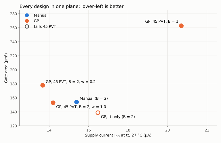
At equal area, the GP design draws 7.7 % less current. Most of the difference is the hand design's spare UGF: 11.5 % above spec at the worst corner, against 1 to 2 % for the GP. The rest is small and spread out: a slightly lower on the input pair, a longer or multi-finger tail mirror, and area placed where the offset needs it.
The most telling row is the last one in the size table. Given the freedom to choose, the GP's NMOS mirror is almost exactly the hand design's: one wide finger, . The operating points agree too. At tt, is within about 1 per device across all three designs: about 23 for the pair, 16 for the PMOS, and 19 to 20 for the NMOS mirror.
Design speed — from hours of SPICE to one verification
A better design was only half of what I wanted from GP. In the first session I asked for this comparison too:
Later, also compare whether designing the OTA with this general GP actually helps over the manual design, in speed as well as performance. On speed, I expect it to help a lot, since it cuts the number of loops.
When Claude first reported the numbers, they mixed up two different things:
Are the counts in this speed comparison all simulation counts? They look mixed with GP iteration counts.
And what is a "round" in the manual design?
So the comparison below uses one unit throughout: SPICE operating-point analyses. Checking one candidate at 45 PVT conditions takes 135 of them, one at the common-mode point and one at each swing end. A "round" of the manual greedy search changes one device group at a time, tries about twelve candidates, and keeps the best. The manual counts come from its logs.
| Manual (greedy) | GP, first PASS (run 11) | GP, final, | GP, final, | |
|---|---|---|---|---|
| Candidates checked at 45 PVT | 131 in 11 rounds | — | 1 | 3 |
| SPICE op analyses | 17,685 | 3,012 | 138 | 414 |
| Fewer than manual | — | 5.9× | 128× | 43× |
| Monte Carlo (mismatch) | final check only | 13 × 1,000 | 1 × 200 | 3 × 200 |
| Wall-clock time | several sessions, partly by hand | about 21 min, automatic | 170 s, automatic | 329 s, automatic |
The manual count is a lower bound. It includes only the greedy run that was kept. With the abandoned first run (zero saturation margin) the total is 43,740. It also leaves out the hand calculations and tt simulations used to find a starting point, and the check after the tail was resized by hand, because none of those were logged.
The reason for the gap is where SPICE sits in the loop. In the manual flow, SPICE is the search: every candidate is a 45-condition simulation, and the greedy search needs a hundred or more of them to settle. In the GP flow the search happens inside the solver, against fitted models that evaluate in microseconds. SPICE moves to the end and only verifies the answer. How often it has to verify depends entirely on model accuracy. Run 11, with coarse models and enumerated lengths, needed 3,012 analyses. Each later fix cut that number: 966 once the tail length became continuous, and 138 once the model was right in the region that mattered. At that point there is one GP solve, one 45-PVT check, and done.
Changing the design is cheap too. Moving the area weight from 0.2 to 1.0 was one command line and five minutes. In the manual flow, a different priority means another greedy run from a new starting point.
Two costs sit outside this table, and both are paid once rather than per design:
- Model extraction. The first five corner models took about 4.5 minutes. The final set is 60 files (5 corners × 3 temperatures × 4 finger widths) and adds the segment and fits; I did not time it end to end. It is per process, not per circuit.
- Building the method. Four sessions went into the formulation, the fits, and the validation described above. That is the cost of the first circuit. The next OTA in the same process reuses the models and the solver and needs only a new circuit file.
Afterwards — was the spec fair?
Near the end I asked whether any spec item was unusually hard compared with typical ones. The answer was the swing: a 50 mV saturation margin with the output only 150 mV from either rail.
A saturation margin of 50 to 100 mV is common, but a 0.15 V output swing limit was a bit tight. Usually it is set to around 0.2 to 0.25 V.
No, never mind. It is a test design anyway, so let us call it an attempt at a tight spec. It cost us some effort, but we learned a lot from it. No need to rerun.
The tightness is what made the model errors visible. At the swing end, a 3 mV error or a 0.15 dB gain bias was enough to decide between and , a 35 % difference in current. A looser spec would have hidden all of them.
What I am taking from this
"Global" means global inside the model and the design space, nothing more. The solver was never wrong. Every time the GP said a design was infeasible, it was right about the problem it had been given. The problem was wrong: a convex fit of a concave curve, a fit dragged by points the circuit never visits, and a finger-width cap that excluded the hand design. A convex formulation turns optimization from a search into a modeling exercise, and the modeling exercise is the hard part.
Measure model error on a design the optimizer did not choose. On the optimizer's own solutions, the gain bias averaged , which looked excellent. On the hand design it was over . An optimizer avoids regions where its model is pessimistic, so checking only its own answers hides exactly the errors that matter. A known-good design is the cheapest independent test there is.
An optimizer finds every optimistic error in a fit. It went straight to –, where the convex fit was most optimistic, and gained 0.6 dB on paper. A fit used for optimization should be judged by its worst residual in the region the optimizer can reach, not by its rms.
EKV gives the right structure, but its parameters are a coordinate system. One formula from weak to strong inversion is what let fit the GP form at all, and one extra term brought it to 2 %. A fitted slope factor of 2.0 is not a physical number.
Keep the global part and make the local part small. Splitting each solve into two pure GPs that bracket the answer, and then SGP fine tuning from the safe side, kept the guarantee where it matters: feasibility and a known gap, instead of a dependence on the starting point.
The speed comes from moving SPICE from search to verification. The hand search ran 131 candidates through 45 conditions; the final GP ran one. That is a 128× cut in SPICE analyses and minutes instead of sessions, and it holds only as long as the model is accurate. Every model error showed up as extra verification rounds.
When the model is right, the correction loop disappears. The SPICE feedback loop was built to absorb model error. Once the device fits were accurate where it mattered, the first GP solution passed and the loop had nothing left to do.
References
- Sizing a Symmetrical OTA on SKY130 in Ten Rounds of Conversation — the hand design this post compares against
- Drawing a Symmetrical OTA in Seven Rounds of Conversation — the schematic
- Optimal design of a CMOS op-amp via geometric programming — Hershenson, Boyd, Lee, IEEE TCAD 2001
- A tutorial on geometric programming — Boyd, Kim, Vandenberghe, Hassibi, Optimization and Engineering 2007
- Convex piecewise-linear fitting — Magnani, Boyd, Optimization and Engineering 2009
- Disciplined geometric programming — Agrawal, Diamond, Boyd, Optimization Letters 2019
- Disciplined Geometric Programming — CVXPY documentation
- Convex Optimization — Boyd, Vandenberghe, Cambridge University Press 2004
- An analytical MOS transistor model valid in all regions of operation — Enz, Krummenacher, Vittoz, 1995 (EKV)
- A gm/ID based methodology for the design of CMOS analog circuits — Silveira, Flandre, Jespers, IEEE JSSC 1996
- Systematic Design of Analog CMOS Circuits — Jespers, Murmann, Cambridge University Press 2017
- Clarabel — interior-point conic solver
- SkyWater SKY130 PDK documentation
- ngspice — open source spice simulator
Disclaimer: This blog post was created with assistance from Claude, an AI developed by Anthropic, under my direct supervision and guidance to ensure accuracy and alignment with my vision for the content.